 23.06.2026Anna Karwowska
Assembly of High-Density Interconnect (HDI) & Ultra-Fine Pitch Components
The success of an electronic product often depends on the physical packaging density of its components and the precision of their assembly. The market sets clear demands: devices must be smaller, lighter, and more functional, while remaining utterly reliable in extremely harsh operating conditions. When a project requires the integration of hundreds of functions within a minimal footprint, standard PCB assembly methods become insufficient.
What are HDI and Ultra-Fine Pitch?
To effectively manage the miniaturization process, one must precisely define technological boundaries and match them with the operational capabilities of the EMS provider.
HDI (High-Density Interconnect)
Transitioning from a classic multi-layer PCB to the HDI standard represents a complete shift in layer architecture and laminate mechanical processing methods. According to the IIPC-2226 (Sectional Design Standard for High Density Interconnect (HDI) Boards), a board qualifies as HDI when the density of connections requires moving away from traditional mechanical drilling in favor of laser methods and sequential lamination.
From the perspective of PCBA processes, HDI components and structures force a complete shift in the approach to Design for Manufacturing (DFM), solder paste deposition precision, and joint quality control. In Assel’s contract manufacturing engineering, this technology is defined by three critical operational areas:
- Trace width and insulation spacing: In advanced projects, we route traces and spaces down to 50–75 µm, enabling the assembly of ultra-fine pitch components. To maintain maximum process stability with such miniaturized structures, we use finer-mesh solder pastes (Type 4 or Type 5) and verify deposition precision using advanced Parmi 3D Solder Paste Inspection (SPI) systems with a 14 µm resolution, ensuring full process repeatability.
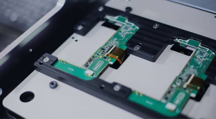
- Via-in-Pad technology: Due to space constraints, microvias (under 150 µm in diameter) are located directly inside the component land patterns. For the reflow soldering process to succeed, these vias must be completely filled with copper or epoxy resin and planarized by the PCB supplier. Assel’s engineering department performs strict Incoming Quality Control (IQC), verifying process correctness based on measurement reports provided by the manufacturer.
- Invisible solder joints: The use of sequential lamination, alongside blind and buried vias, means that critical connections remain hidden from the naked eye. At Assel, automated 3D Optical Inspection (AOI—Parmi systems with 14 µm resolution and VI systems with 19 µm resolution) combined with advanced 3D AXI X-Ray inspection have become standard practice, enabling non-destructive verification of microvias and solder joints underneath array packages.
Ultra-Fine Pitch
While HDI defines the geometry of the bare board itself, Ultra-Fine Pitch refers to the extreme miniaturization of component terminations. According to the IPC-T-50 classification, components with a pitch between 0.65 mm and 0.5 mm are considered Fine Pitch. The Ultra-Fine Pitch threshold begins below 0.4 mm.
In mass serial production at Assel, we successfully assemble 0.35 mm pitch packages, and our advanced machinery park is technologically fully prepared to handle even finer pitches—down to 0.3 mm and 0.25 mm. Designing and assembling components in this class primarily involves three package types:
- Micro-BGA (µBGA): Array packages where the solder sphere diameter is a mere 150–200 µm, drastically reducing the margin of error for repeatable paste deposition.
- CSP (Chip Scale Package): Packages whose physical footprint does not exceed 1.2 times the area of the silicon die. This minimizes thermal mass and alters the component's dynamic behavior inside the reflow oven.
- WLCSP (Wafer Level Chip Scale Package): The most uncompromising form of miniaturization. Solder balls are attached directly to an uncut silicon wafer. The component reaches the SMT line without any additional packaging, placing extreme demands on Pick & Place systems.
To meet these requirements, Assel’s production lines are equipped with flagship ASM SX2 and ASM X4S placement machines. They allow us to achieve top-tier component positioning accuracy: up to ±26 µm at 3σ in the X/Y axes, and ±0.05° at 3σ angularly.
Technological Synergy
These two concepts cannot be separated. Attempting to implement an Ultra-Fine Pitch component (e.g., a processor in a 0.35 mm or smaller WLCSP package) onto a standard, non-HDI board is physically impossible. Component miniaturization directly forces a change in PCB technology—routing signals out of dense-pitch ICs requires Via-in-Pad technology, blind microvias, and ultra-narrow traces.
Design Challenges and the Role of DFM Engineering
Although designing high-density layouts rests with the OEM, the physical realities of assembly frequently necessitate adjustments to the documentation. Assel’s DFM engineers—working with advanced Valor software—support clients during the very first stages of design review to identify manufacturing risks that could compromise assembly stability across three key areas:
- Thermal Management: We pinpoint risks tied to dense component packaging that can hinder the reflow process (e.g., uneven temperature distribution across the board), ultimately affecting solder joint quality.
- Signal Integrity and EMI: We verify documentation against real-world manufacturing capabilities, paying close attention to minimum insulation gaps; exceeding these thresholds can create barriers to achieving high process repeatability.
- Mechanical Stress: We evaluate designs for their susceptibility to warpage. We flag the placement of sensitive packages (BGA, CSP) in high-stress zones to minimize the risk of joint micro-cracking as early as the assembly stage.
Strategic PCB Approach and Advanced Laminates
Traditional printed circuit boards rely on through-hole vias, which block routing channels across all layers. HDI technology redefines this structure using laser-drilled microvias:
- Blind Vias: Connect outer layers to inner layers without going all the way through the board.
- Buried Vias: Connect inner layers exclusively.
- Stacked Vias: Placing microvias directly on top of one another, enabling vertical signal transmission with a minimal surface footprint.
Working with Ultra-Thin Laminates: Any-Layer HDI and SLP
Modern circuit boards increasingly rely on Any-Layer HDI (ELIC – Every Layer Interconnect) and SLP (Substrate-Like PCB) architectures, where trace widths drop below 30 µm. From a contract manufacturing standpoint, these laminates pose a massive operational challenge—lacking a traditional rigid core, they are exceptionally thin.
At Assel, we successfully process laminates as thin as 0.35 mm. Such flimsy boards are highly prone to mechanical and thermal deformation at every stage of the SMT line. Without proper support, the board's flexibility would make it impossible to maintain the required precision during solder paste printing and component placement.
To prevent this, our in-house team of mechanical engineers designs fully customized, proprietary carrier pallets, which we manufacture ourselves using Assel’s internal CNC machine park. These fixtures stabilize the 0.35 mm board throughout the process, drastically reduce mechanical stress, and guarantee perfect board flatness, translating into maximum reliability for the finished product.
Via-in-Pad Technology (VIPPO) and Supplier Control (IQC)
Using the VIPPO (Via-in-Pad Plated Over) technique—placing a microvia directly inside a solder pad and plating it over with metal—is standard practice today for BGAs with a pitch below 0.5 mm. While it reduces parasitic trace inductance and saves space, the quality of this connection is determined long before the assembly itself.
PCB design and via execution represent a critical checkpoint. That is why Assel places immense emphasis on rigorous Incoming Quality Control (IQC) of bare laminates. For every production batch delivered by PCB suppliers, we verify:
- Metallographic cross-section reports and samples,
- Pad solderability tests,
- Layer stackup compliance and controlled impedance (where applicable),
- Correctness of structural execution against the design (e.g., selecting the appropriate via plugging and filling type per IPC-4761).
Inaccurate epoxy filling or faulty copper plating by the PCB fabrication house risks trapping air or causing solder paste "wicking" down into the via during reflow. This leads to dangerous voiding and structurally weakened solder joints.
Base Material Selection
Assembling electronics onto standard rigid laminates (FR4) or flexible/hybrid circuits (Flex, Rigid-Flex) is an excellent solution for systems requiring efficient heat dissipation.
However, when entering the realm of dense HDI structures, standard laminate grades must give way to advanced variants. For rigid laminates, the use of high glass-transition temperature resins (High Tg $\ge$ 170°C) with a reduced Coefficient of Thermal Expansion (CTE) in the Z-axis becomes mandatory. This specification prevents delamination and microvia cracking under the thermal stress of SMT reflow. Furthermore, any material operating at such fine pitches must offer absolute resistance to CAF (Conductive Anodic Filament) growth, an electrochemical copper dendrite phenomenon that threatens micro-shorts.
Production Line Challenges: SMT Assembly
Dropping down to 0.35 mm pitches pushes the SMT process into a territory where physicochemical parameters become critical. The greatest challenge lies in the highly repeatable deposition of microscopic volumes of solder paste.
Solder Paste and Stencils
The primary physical metric monitored on the SMT line is the Area Ratio (AR). For the solder paste to release correctly onto the pad, we maintain a strict mathematical condition:
$$AR = \frac{\text{Area of Aperture Opening}}{\text{Area of Aperture Walls}} > 0.66$$
For Ultra-Fine Pitch components at Assel, we use high-precision laser-cut stencils, tailoring solutions to individual project demands—including advanced step-up and step-down stencils for more complex layouts. These allow us to locally vary stencil thickness, optimizing paste volume for both dense-pitch ICs and larger components on the same PCB. We work primarily with proven Alpha Type 4 (and occasionally Type 5) solder pastes.
Process repeatability is guaranteed by 100% SPI inspection, which verifies paste deposition across every single manufactured board; paired with full traceability, this offers absolute oversight of the process. Thanks to stencil precision, tightly controlled print parameters, and continuous SPI feedback, we eliminate the need for stencil nano-coating in serial production.
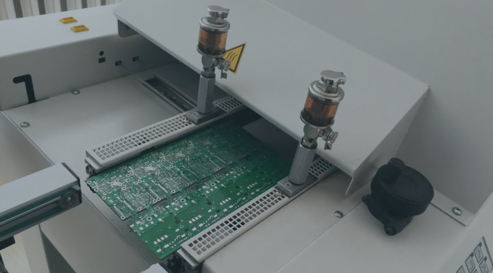
Thermal Dynamics and Reflow Profiling
Small passive components (such as 0201 packages) heat up exponentially faster than massive integrated circuits. At Assel, our thermal profiling relies on advanced, multi-point measurement using an 8-channel KIC K2 calibration system.
For lead-free SAC305 alloy profiles, we control temperatures strictly: we typically design peak temperatures at 241°C, taking absolute care never to breach the 245°C mark. This minimizes the temperature delta ($\Delta T$) across the PCBA surface (the exact $\Delta T$ depends on the specific design and copper distribution), preventing two critical defects:
- Tombstoning: The lifting of one end of a small passive component due to unbalanced solder surface tension.
- Warpage: Laminate deformation resulting in cracked vias or open BGA joints.
Our reflow ovens possess the technical capability to solder under a nitrogen ($N_2$) atmosphere. However, standard thermal profile optimization at Assel is sophisticated enough that continuous $N_2$ blanketing is rarely necessary in serial HDI production. It is also worth noting that while we do handle low-temperature (BiSn) solder pastes, we reserve this process for specific, non-HDI applications.
Mechanical Reliability in Production: The Underfill Process
Even a flawlessly executed reflow process for Ultra-Fine Pitch components is sometimes not enough to guarantee a device's ultimate resistance to vibration and physical shock in its end-use environment. Solder spheres measuring ~150 µm are subjected to immense shear stresses.
To counteract this, we implement the Underfill process in serial production—dispensing a specialized capillary resin underneath the packages. At Assel, this is executed via highly precise, repeatable manual dispensing using CTE-optimized resins from renowned manufacturers like Loctite/Henkel. Once the resin is applied beneath the IC, the boards pass through a strictly controlled tunnel curing process. This assembly expertise binds the silicon and the laminate into a single monolithic block, elevating the mechanical reliability of the finished device to the highest possible level.
Quality Control, MSL Management, and Full Traceability
Standard optical inspection faces severe limitations in HDI layouts—cameras cannot see underneath BGA or CSP packages. Therefore, Assel’s standard quality gate for advanced PCBA projects relies on a three-stage verification system:
3D SPI (Parmi) $\rightarrow$ 3D AOI (Parmi/VI) $\rightarrow$ 3D AXI (X-Ray)
X-Ray inspection is the only tool capable of non-destructively catching the extremely dangerous Head-in-Pillow (HiP) defect. This occurs when a BGA sphere maintains physical contact with the solder paste (e.g., due to thermal warpage) without actually coalescing into a single metallurgical joint. Such a connection may pass In-Circuit Testing (ICT), but is virtually guaranteed to fail in the field.
IPC Standards and Strict MSL Oversight
Assel carries out assembly operations based on the process guidelines of the J-STD-001 standard (which dictates rigorous methods and requirements for manufacturing and soldering processes), while final inspection and board acceptance are conducted strictly according to IPC-A-610. We routinely manufacture to Class 2 and the highly stringent Class 3, adapting criteria to custom contractual agreements.
A vital element in protecting dense-pitch components (BGA/WLCSP) from "popcorning" damage during reflow is Moisture Sensitivity Level (MSL) management. We operate in strict compliance with the IPC/JEDEC J-STD-033 procedure. We maintain low-humidity dry/nitrogen cabinets for safe storage alongside dedicated component baking ovens. Crucially, tracking component floor life exposure is integrated directly into our Pick & Place machines to automate MSL compliance oversight.
Case Study 1: Medical Sector
In one medical project, the main hurdle proved to be the process complexity generated by cutting-edge assembly methods and PCB construction. The project involved integrating components in a Package-on-Package (PoP) architecture on multi-layer HDI boards. The manufacturing flow demanded ultra-precise manual soldering of peripheral components alongside strictly controlled underfill application. While the specific laminate behavior and microvia requirements posed a severe challenge during bare PCB fabrication, Assel’s refined process procedures allowed the final product to pass rigorous testing and operate flawlessly in medical applications.
Case Study 2: Optimizing PCB Surface Finishes
In another serial project spanning the MedTech and industrial automation sectors, Assel’s engineering team suggested changing the bare board surface finish from traditional HASL to ENIG (Electroless Nickel Immersion Gold) during the DFM phase. The uneven topography of a HASL coating on ultra-fine pitch pads generated high risks of solder bridging and placement planarity issues on our ASM machines.
Switching to ENIG yielded twofold benefits: it provided perfectly flat pad surfaces (exceptional fine-pitch solderability) and completely eliminated the issue of bare boards "expiring" in warehouse storage, boosting the customer’s operational flexibility. This single engineering recommendation allowed the client to eradicate assembly defects entirely.
Summary
As an agile EMS partner, Assel focuses on our clients' real-world manufacturing needs and uncompromising process repeatability.
Our competitive edge on the European market is built around engineering flexibility and unique know-how in stabilizing difficult production flows. While standard practice at many EMS plants involves dodging ultra-thin laminates or outsourcing tooling, we design and machine our own carrier pallets in-house, custom-tailoring them to prevent thermal warpage in 0.35 mm packages. Pairing a top-tier ASM machinery park with three-stage automated inspection (3D SPI + 3D AOI + X-Ray) and dedicated, software-driven MSL floor life tracking ensures that Assel delivers predictable, world-class PCB assembly services.