The customer's desired situation would be the delivery of a batch of products without any faulty copies. Therefore, many technological solutions related to quality control are used in practice. One of such systems is AOI, i.e. automated optical inspection. It allows to quickly check the correctness of PCB assembly.
Reliable quality control brings many benefits, such as:
- Lower cost. The faster a defective part is discovered, the lower the cost to repair it.
- Customer trust. To build long-lasting relationships with customers, it is essential to eliminate defective pieces from delivered batches.
- Improving the production process. By verifying the errors that arise, you can improve the process to get more correctly assembled boards in the future, which will translate into better financial results.
For these reasons, every PCB assembly process should also have control systems such as AOI.
What is automated optical inspection?
PCB assembly is a complex process in which many different operations are performed. Human control of PCB assembly is limited by repetition and time constraints. Automated systems come to the rescue. AOI allows real-time comparison of the assembled PCBs with the pattern in order to detect errors. A distinction is made between 2D and 3D automated optical inspection devices.
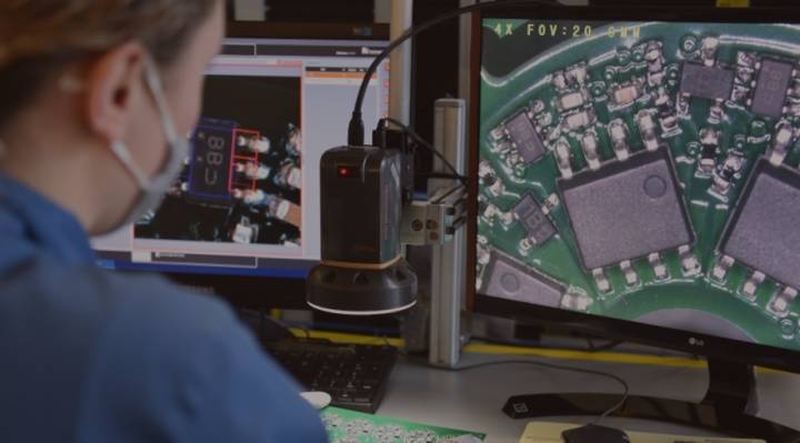
Older 2D systems took a picture of the finished board and compared it to a reference picture stored in the memory of the device. On this basis, deviating PCBs were detected. Additionally, it performs vector measurements, increasing the efficiency of quality control. In the case of 3D systems, additional laser measurements are added to the image, which allows to obtain a spatial image of the PCBA. Thus, three-dimensional systems are an improved version of two-dimensional systems, which allows them to detect errors impossible to find with 2D methods.
With the help of AOI systems, not only the PCB assembly, but also the inspection, can be fully automated. They allow for ongoing production control and error detection. They also make it possible to perform pass/fail analysis. All boards found to be faulty are redirected to the controller, who definitively verifies a given board.
How does automated optical inspection work?
As already mentioned, the first was 2D automated optical inspection, which then evolved to 3D. Even 2D technology has proved revolutionary for post-assembly inspection of PCBs. Why? It allowed a very fast production inspection when compared to regular workers. It made it possible to test all assembled PCBs, not just selected samples.
The machine takes a picture of the finished PCB and then compares it to the stored pictures of the components. The 2D AOI compares individual pixels to each other, so it can easily detect defects such as rotation, polarity, bridging, missing component, or the wrong component in the right place (dimensionally different). More advanced models can also read individual component markings.
The use of the laser to create 3D images of the assembled boards also allows the detection of lifts, tilts, bad solder leads or tombstone effects in the case of chips. This wide range of testing makes AOI systems the perfect solution for PCBA assembly.
Advantages of AOI
PCB assembly currently requires continuous real-time inspection by AOI systems. Such solutions are widely used today because they offer numerous advantages:
- Detection of the smallest errors. The components used in PCB assembly are getting smaller and smaller. To achieve high enough sensitivity, the AOI system must have sub-pixel accuracy.
- Fast detection of defective boards. The faster an AOI system identifies defective wafers, the lower the cost to repair them. This does not only apply to individual pieces. In the case of serial faults, catching the defect at the earliest possible stage is key to minimising costs. Potentially defective pieces are assembled all the time. Automated quality control makes it possible to interrupt production very quickly and make the necessary corrections.
- Flexibility. The PCB assembly is a multi-stage process. Automated optical inspection can be used at any stage of the production line, which increases the usefulness of this technology.
- The AOI system accurately detects specific and programmed errors made during PCBA assembly. The very high efficiency is certainly the most important advantage of this system.
The use of AOI is therefore very beneficial in the PCB assembly. This translates into eliminating serial errors at an early stage and eliminating virtually all defective pieces.
Why is AOI an integral part of PCB assembly?
By using AOI systems in PCB assembly, individual components can be positioned with a high degree of accuracy to determine which boards are defective. This reduces the cost of repairing them, and eliminates serial errors at an early stage of production. At the same time, it has a positive impact on the quality of subsequent batches. This technology is also very fast, which increases the production capacity and efficiency of the entire system. The flexibility of such equipment, light control and the possibility of programming the relevant parameters allows for optimisation of control.
AOI ensures a high quality standard, but it cannot detect all types of errors made during PCB assembly. Therefore, it is often used together with other systems such as:
- SPI (Solder Paste Inspection).
- AXI (Automated X-Ray Inspection).
The use of several inspection systems ensures the highest quality of the produced PCBs. It enables the detection of defects invisible to the naked eye.


