 10.03.2021Przemysław Prolejko
Reliably conducted assembly of printed circuit boards means not only a smooth transition through all phases of production but also watching over the course of the process and its quality at every stage. Implementing and maintaining product control procedures holds a number of benefits for the employer:
- Cost – both the measurable one (lower risk of introducing a bad product to the market, which will then have to be withdrawn) or the incommensurable one (once a brand's reputation is lost, it is difficult to rebuild it), and the time saved (for example, in the context of longer waiting time for another correctly executed delivery).
- Product tolerance range – the finished product is intended to serve in specific conditions, and thus, it is supposed to meet specific requirements, e.g., regarding the device's response at a given temperature (hot/cold), resistance to interference, or noise emission. These are important because of the class of the final product that the circuit board will be a part of.
- Quality verification and error detection – primarily during final production. These actions are critical in the context of preventing defects or problems early in the life cycle of the final product.
Therefore, depending on the product specification received when performing SMT assembly, a good contract electronics supplier will apply a number of inspections and tests that will verify the product in a multi-faceted manner before it is handed over to the contractor.
Inspection of PCB assembly
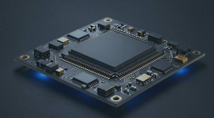
An inspection is simply an examination of a product, including its design or manufacturing process, and determination of its conformity with specified or general requirements (based on professional judgment). The assembly of printed circuit boards can be subject to a multi-faceted assessment, depending on the specific clients’ needs.
Inline Automated Optical 2D and 3D Inspection (AOI)
It is a method used to identify problems early on. This allows you to pause production to reassemble the circuit boards after correcting the identified deficiencies.
Automatic visual inspection of the PCB is performed with the use of a 2D or 3D camera and by performing a laser measurement. Cameras take pictures of the board, which are compared by the system to a previously uploaded detailed product diagram. If the scanned plate does not match the schematic in any way, it is marked for the technician's inspection.
SMT assembly controlled by the AOI system can be prevented from critical errors (e.g., missing component) and quality defects (e.g., crooked components). This type of review can also catch very small flaws, such as scratches in the stacked parts or polarization.
Please note that this inspection is based on visual aspects only, so it will not verify the functionality or compatibility of the used elements.
3D Automated X-Ray (AXI)
This is another of the diagnostic methods for early fault detection. During this test, an X-ray technician (who is a trained and experienced operator) is able to locate invisible defects concerning, among others, proper distribution of solder paste under the components (e.g., BGA) or connections with solder joints under the chip package.
X-rays automatically scan the plate and find errors that are not visible during visual inspection.
This allows for each layer of the plate to be X-rayed to detect internal defects. However, it is not always cost-effective to perform 100% product inspection – it is an expensive process, so the scope of the test is agreed upon in advance with the client or performed periodically to check the stability of the process.
3D Automated Solder Paste (SPI)
This is a fast and precise method of inspection. The solder paste inspection serves to detect errors associated with improperly applied solder paste.
It is performed with the use of dedicated apparatus with vision sensors, which analyze the level of the printed solder layer (whether it was applied in the right amount and spread evenly) after applying the solder paste in the screen printing process, and before placing the components on the PCB.
Manual/Visual Inspection
Depending on the contract electronics supplier's procedure, those may occur at different stages of the production process.
The PCB assembly is then verified manually by the operator using visual assessment or dedicated fixtures (e.g., poka yoke). An inspection may involve checking solder paste after printing, components after they have been placed on their target PCB locations, or solder joints after the solder has cured.
This type of inspection is the least repetitive, with no need to purchase additional specialized equipment to perform the inspection.
PCBA assembly tests
In contrast to inspections, which are mainly based on the visual evaluation, tests consist of practice tests, when the assembly of printed circuit boards reaches its final stages, in order to check the properties and operation of the finished or nearly finished product (which can still be subject to possible corrections before handing it over to the client).
Functional tests (FCT)
This is a desirable form of verification – it is performed on the finished product to verify that the product works – it will turn on, it performs the expected function, and that all the components work together in a cohesive manner.
SMT assembly, and in fact the final product, is tested in this respect in consultation with the client and with their participation during the construction of the testing environment. These are dedicated test fixtures built specifically for a given product. The client supplies a ready-made solution, or a good PCB assembly contractor constructs it to order.
Preparing a test for a given product is time-consuming, extends the production cycle, but at the same time allows for a fully qualitative approach to the goods offered to the client (building your own image as a manufacturer offering quality and durable products), as these attributes are checked before releasing the final device on the market.
ICT tests
In-circuit test. Quick and automatic tests to detect potential assembly errors, such as those resulting from the use of the wrong component, reverse polarity, the presence of short circuits or interruptions. They are performed before the functional test, when the SMT assembly enters the final stages, assuming the possibility of possible corrections to the "mature" product.
To perform the test, a dedicated PCB matrix with appropriately spaced gold-plated needles is used, through which an electrical signal is transmitted to individual components, checking the integrity of the solder joint.
Safety tests:
- Burn-In Test – a test designed for early failure detection and determine the finished PCB's maximum performance.
The test involves leaving the finished kit in a special room with a high temperature continuously for 48 to 168 hours. If the system is damaged, this is known as infant mortality.
Performing this test prevents a troublesome or dangerous product from being introduced on the market. At the same time, applying increased load may shorten product life or damage some components, so if intensive testing shows few or no defects, testing conditions can be reduced to avoid unnecessary overloading of the PCB.
- Hi-Pot PCB Testing (High Potential/high voltage test) – this test is recommended for high voltage PCBs and when thin dielectrics are used in the design.
The test verifies that the dielectric material of the PCB can withstand a voltage higher than the rated voltage without damage (voltage spike). The high voltage is passed to the board for a few seconds (hence this test is the opposite of a continuity test).
It is a non-destructive test that determines the adequacy of electrical insulation for a normally occurring transient voltage. It is used to confirm that the insulation used is not marginal and that inadequate leakage paths and clearance distances were not created during the manufacturing process.
Environmental testing
These tests check the conformity of the constructed product with the relevant standards for functionality, safety, and durability within the product specification declared by the manufacturer.
Depending on your needs, these tests may require a different diagnostic kit. The basic equipment needed to carry out this type of research includes temperature and humidity chambers or thermal shock chambers.
These tests help accelerate the aging process to predict the life cycle of a product, analyze the types of failures, and filter out those products that are not suitable for shipping to clients.