 22.05.2020Przemysław Prolejko
Introduction to Electronics Assembly
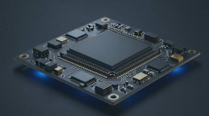
Surface mount technology (SMT) is an electronics assembly production process in which the electronic components such as resistors, transistors, ICs etc. are mounted (by soldering) directly onto the surface of a printed circuit board (PCB). This method gives a variety of benefits like:
- smaller size and weight of final product,
- electrical noise reduction
- speed up of the electronics production process
- decrease of potential reliability defects
In consequence, the SMT reduces manufacturing costs and uses PCB surface area more efficiently than it’s predecessor: through-hole technology (THT).
Nevertheless SMT is not a zero-defect process and due to the components miniaturization and high density of them on the PCB area, repair of potential errors becomes much more difficult, and this becomes valid especially when the defect is detected at the final stage of the assembly process.
To avoid such undesirable incidents it’s necessary to implement high quality inspection. This ensures that the PCB assembly has no defects and is eligible to leave the SMT production line to further manufacturing processes. Clearly, manual inspection is not the most desirable solution for a complex electronic devices and a high volume production environment. The main reason is the inspection time of a single PCBA (Printed Circuit Board Assembly), which is economically unjustified.
Therefore, a good electronics manufacturing services provider (EMS), would use an automated optical inspection (AOI) solution. AOI enables fast and accurate inspection of electronic assemblies and in particular PCBA’s - to ensure optimum quality.
What is AOI and what does AOI inspect?
Automated optical inspection (AOI) uses optics to capture and analyze images of a PCB to verify the following for assembled electronic components:
- presence and position
- soldering (solder joints and bridges)
- polarity
- marking (like inscription, signs, color etc.)
- flux deposits
- microcracks and subsurface defects
It’s an extremely powerful solution to identify defects and ensure the quality of the manufacturing process. AOI systems are placed just before (a more infrequent concept) and just after the soldering process (a very frequent solution) in a surface mount line. An electronics manufacturing provider that is focused on reliable assembly services, would utilize two AOI’s in one SMT line mainly for complex, advanced products that require in-depth inspection.
Depending on the inspection goals, which the AOI manufacturer wants to achieve, the AOI machine may be equipped with:
- one or more high-definition or infrared cameras
- multiple light sources like: UV fluorescence lighting, LED lighting or infra-red.
Images made by the optical solution are sent to the computer and analyzed by complex algorithms built by the equipment manufacturer. This algorithm is the heart of whole inspection system – and compiled with expected results of a particular feature / attribute (like component body size, solder joint brightness etc.). Based on that, differences, abnormalities or even errors can be clearly indicated by its built-in processing software. Besides, all inspection results for all PCBs can be recorded in a database, which allows the contract manufacturer to in-depth measure and analyze production quality results.
Types of AOI systems and Capabilities:
Both 2D and 3D AOI inspection systems are available on the market. However, 3D inspection has allowed more accurate measurements and a more stable inspection process over 2D inspection.
2D AOI Systems:
2D inspection technology, which is less expensive than 3D AOI, is the most common solution used by contract manufacturers and OEMs. There are several 2D AOI systems available on the market. The most advanced systems among them have multiple high-resolution cameras (8 to 15 MP resolution) and precise lenses. They also use sophisticated inspection algorithms to inspect defects.
2D systems offer a wide range of performance features:
- Flexible inspection capabilities
- Optical character recognition and verification (OCR, OCV)
- Data matrix code reading
- Straightforward recognition of certain polarity marks
- Less susceptible to shadowing issues
- Multiple solutions for additional tasks beyond solder joint inspection, such as measurement tasks or color analysis.
However, 2D technology also has limitations such as it cannot inspect hidden solder joints and provide volumetric measurement data (required to measure coplanarity and solder volume/shape). Furthermore 2D AOI shows higher level of false defect rates compared to 3D machines.
3D AOI Systems:
The 3D AOI is available on the market since only a few years, and has been adopted by more advanced and experienced electronics manufacturing providers. The main advantage of an 3D inspection over 2D inspection within the PCB assembly process, is that it provides true volumetric height information. It can measure the volume of each and every visible solder joint of every component. Coplanarity on lifted leads and other height-sensitive devices can be detected without difficulty. Since height data can be measured, AOI programmers can specify the precise height tolerance acceptable for a particular component. Thus, in summary 3D AOI systems can:
- measure volumetric inspection data
- perform true coplanarity inspection
- reduce false call rate
Despite this, 3D AOI technology also has some drawbacks. More engineering programming work is involved in the process of defect detection, which drives up associated costs. In addition, the edges under the components are not analyzed, shadowing problems still occur, there is no evaluation of hidden solder joints with classification of each individual joint, and high components can only be inspected to a limited degree.
Advantage of 3D AOI Systems over traditional 2D AOI Technology:
Since 2D systems deploy light from multiple angles onto the PCB, components and solder joints, all results for inspection are dependent on either contrast or location of reflection points.
Even when multiple camera or viewing angles are used, the results are still based on the availability of the applied light. Hence taller components will cast shadows onto other components and solder joints. The different lighting conditions resulting from shadowing require the AOI programmer to modify thresholds on a component-by-component basis.
As the same type of components on the same board have different thresholds applied, this leads to different defect detection capability and varying amounts of false calls. An alternative way, would be to modify the inspection program and add more pictures, for instance from directly above the inspected component, which eliminates shadow effect, but increases the inspection time.
There are technological factors that make either a 2D or a 3D AOI system a better choice for a given application. However, there are other factors to consider, such as cost and the intended use of the PCB assembly. In reality, 3D AOI technology is indeed the more powerful and advanced technology, where traditional 2D AOI inspection cannot provide the measurement capability required for quality assurance. 3D measurement technology is the perfect process optimization solution for ensuring better quality products. An experienced EMS offering SMT assembly for demanding markets would definitely opt to implement such solution at its facilities.
What other inspection systems should a good electronics manufacturing services provider have in place?
Solder paste inspection (SPI) is another method used within the SMT assembly line in order to ensure the desired amount of solder paste has been deposited to the respective solder pads without any defects. SPI can also measure warpage of PCB, which can be helpful to inspect PCB’s before production. Latest SPI machines can also work in a closed loop with the solder paste printer as a self-optimized process – when the SPI machine get PCB with printed paste, start measure volume, position and height and based on that can change printer parameters to ensure good printing quality.
Automated X-ray inspection (AXI) is another handy inspection method that we need to consider in PCB assembly production. As we have discussed earlier both 2D and 3D AOI technology cannot have the ability to inspect under a certain component and this is quite necessary for components such as QFN and BGA packages. Because the solder points are placed under the IC it is not possible to check them with regular cameras. In such cases X-ray vision allows to detect hidden solder joints. Such inspection also can detect voids in solder joints or solder bridges between solder joints.
Why is inline AOI within the SMT process important?
Based on the above information we conclude that where AOI is concerned, using a combination of 2D and 3D technology is the way to ensure better detection of all visible defect features. If in addition, an in-line SPI machine is adopted, including an X-ray (AXI) inspection capability, one can build a very reliable , automated inspection system for demanding PCB assemblies .
The ideal solution for a smart electronics manufacturing factory is to use various elements from the 2D AOI, 3D AOI, SPI and AXI toolkit to build optimized solutions that meet customer-specific requirements in different phases of production. The major value of smart factories comes from experience, investment in technology, as well as developed software solutions for managing the production process. To achieve the above, the best smart factory quality control solution in the electronics manufacturing environment is the combination of human brain power (organizational and engineering capabilities) and algorithms. In this way we can considerably improve both inspection quality and manufacturing processes.